Recall from the last post that the USB port wasn't able to be automatically placed on r1 due to a mistake I made in the PCB boundary. This is a log of the steps needed to place the part manually.
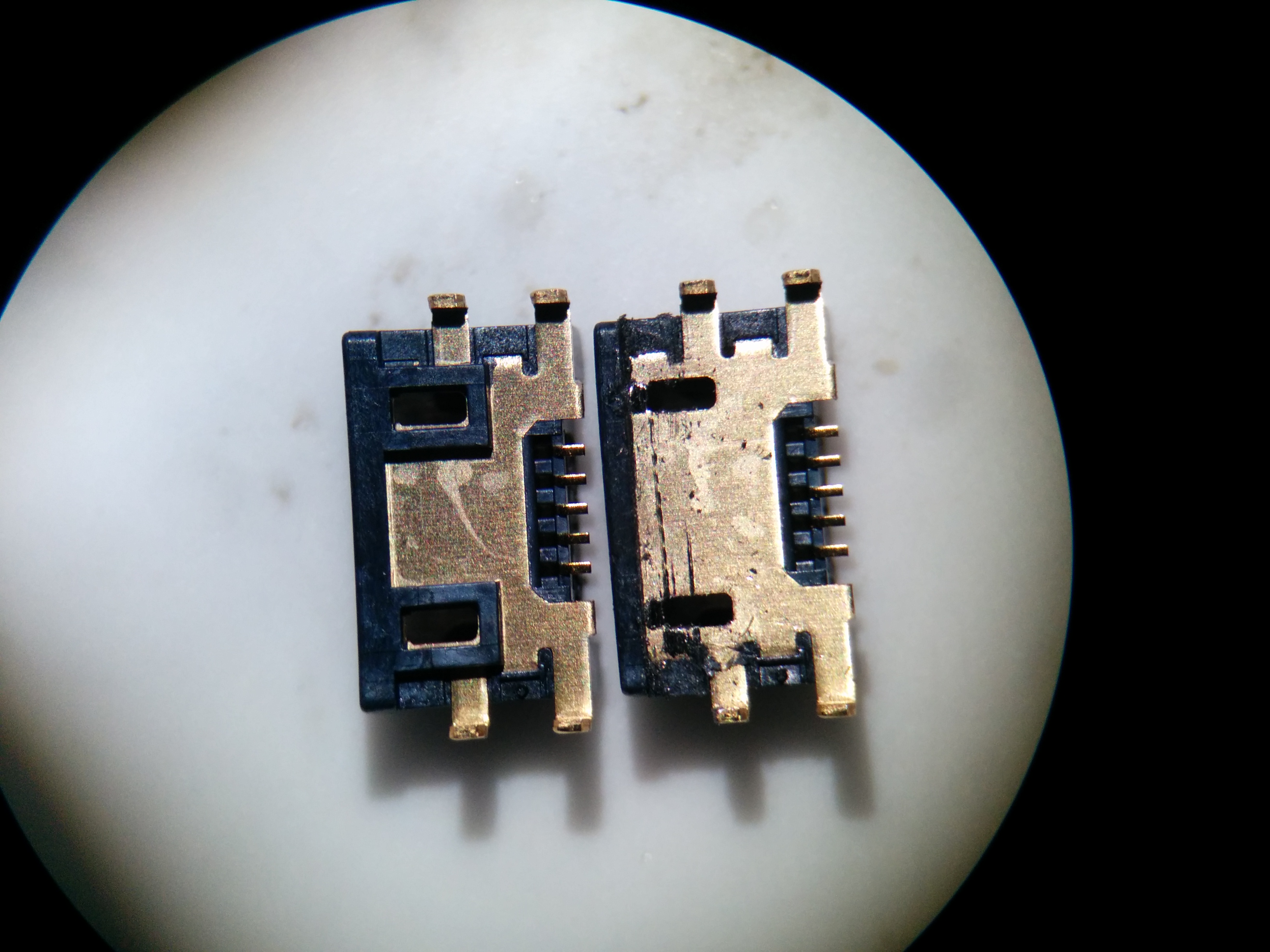
First, I'll prep the connector. The reason the PCB needed to be routed was to accommodate the features on the bottom of the connector. So I need to cut those features off. The modified connector is on the right. You can see marks where my file struck the metal housing.
Since the board was re-flowed and the solder-mask wasn't altered to account for the missing part, I need to remove the existing solder. Normally, I would use flux and braid to do this, but since those pads are essentially ground plane, the heat-sinking would make desoldering a nightmare. I opted to shave down to the pads instead. Here is a pic with two of the grounding pads shaved.
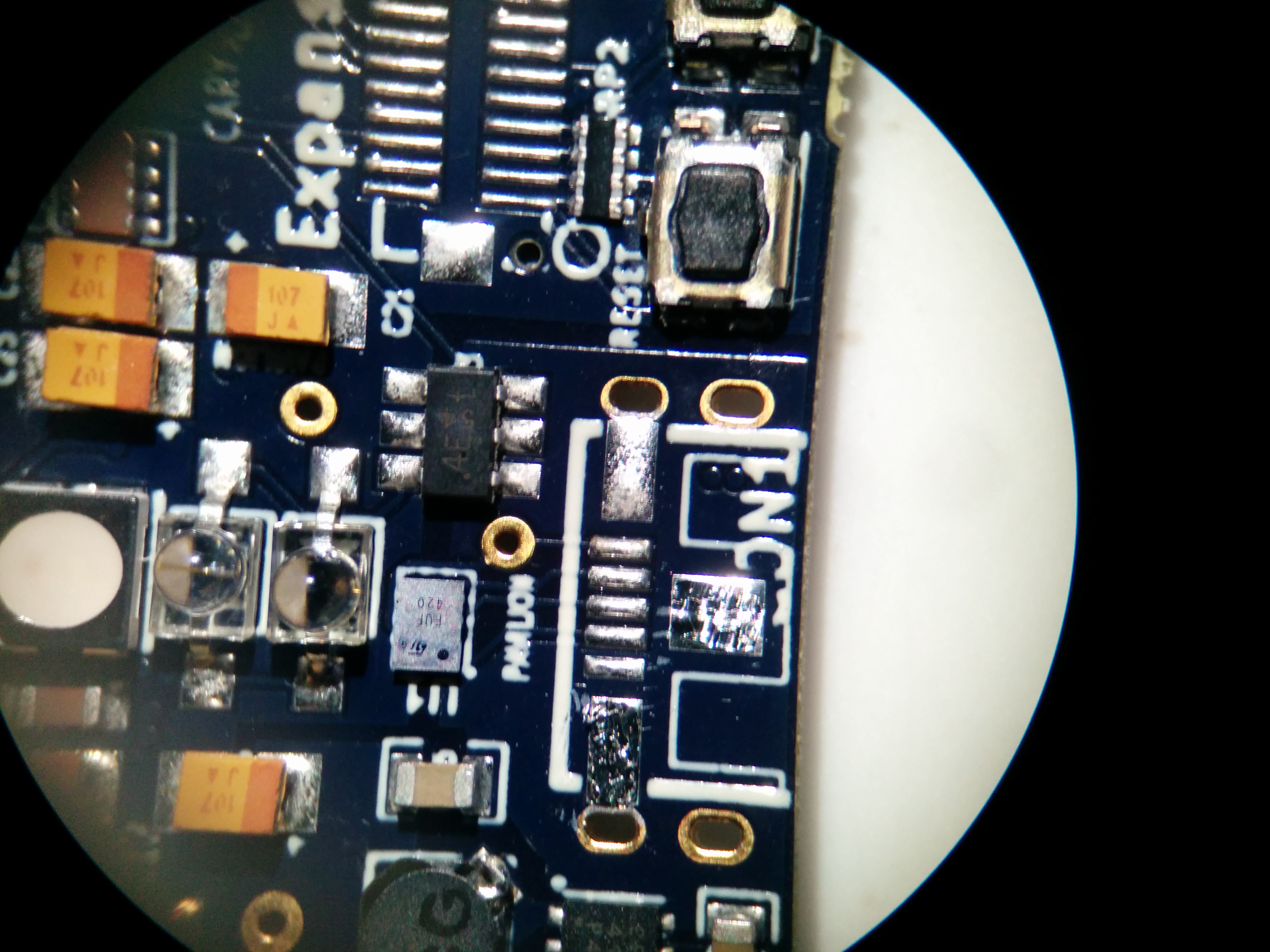
I'm not going to attempt connection of the large ground pad under the connector. Some of it will re-flow and connect, but without being able to hit the pad with heat directly, I don't want to risk the parts on the other side of the PCB coming undone. So once the pads are shaved, fill the slotted holes with solder paste...
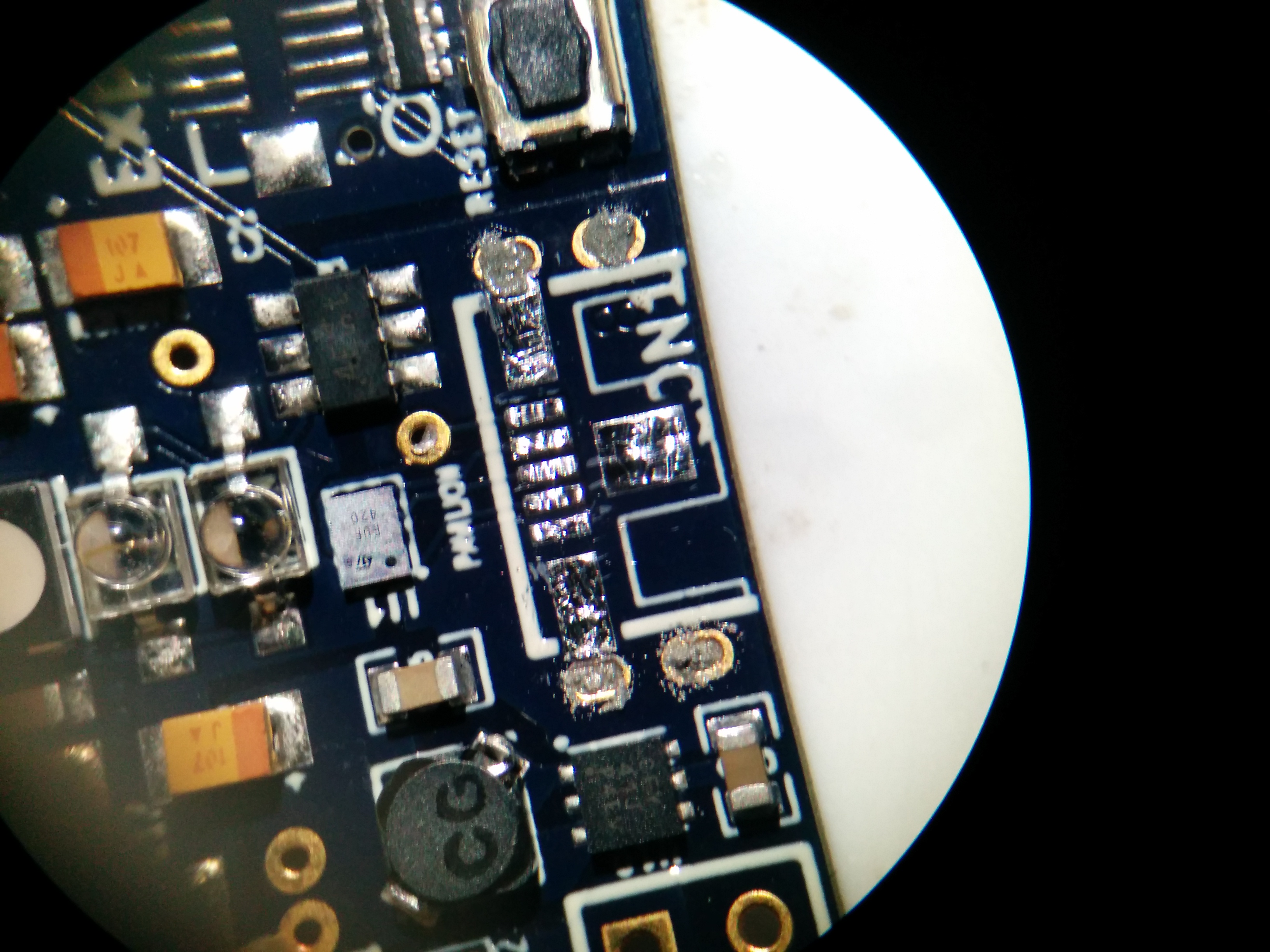
Then, place the connector, solder the slotted holes, and tap each of the USB pins with the iron to re-flow them with a dab of paste...
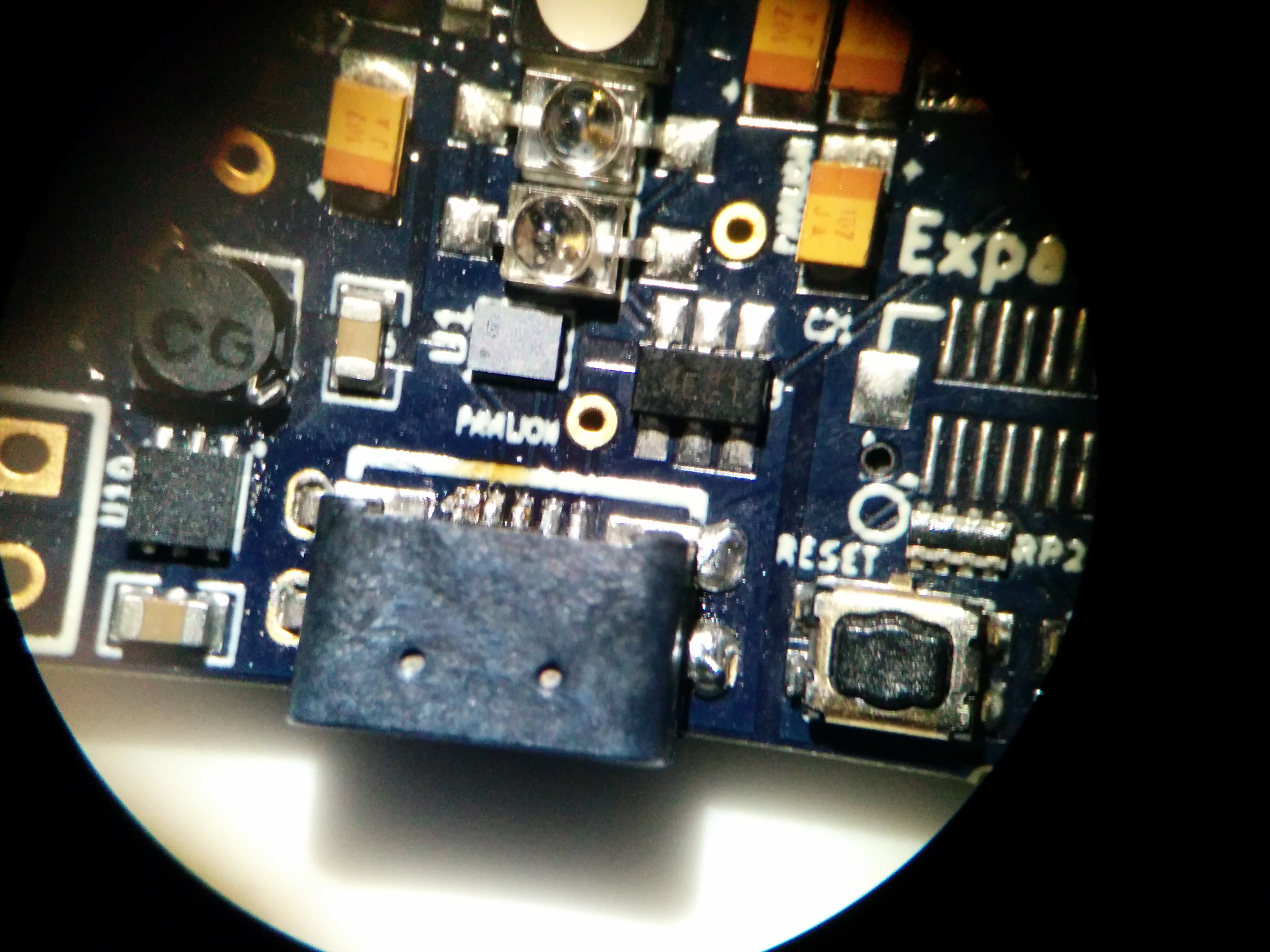
Continuity tests good. Host PC enumerates the device. Repair complete.