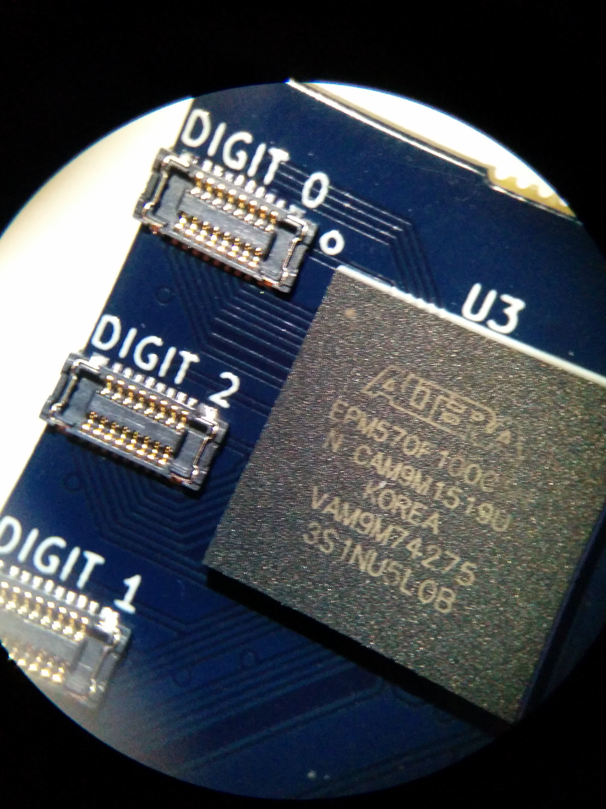
October has been a busy month for hardware...
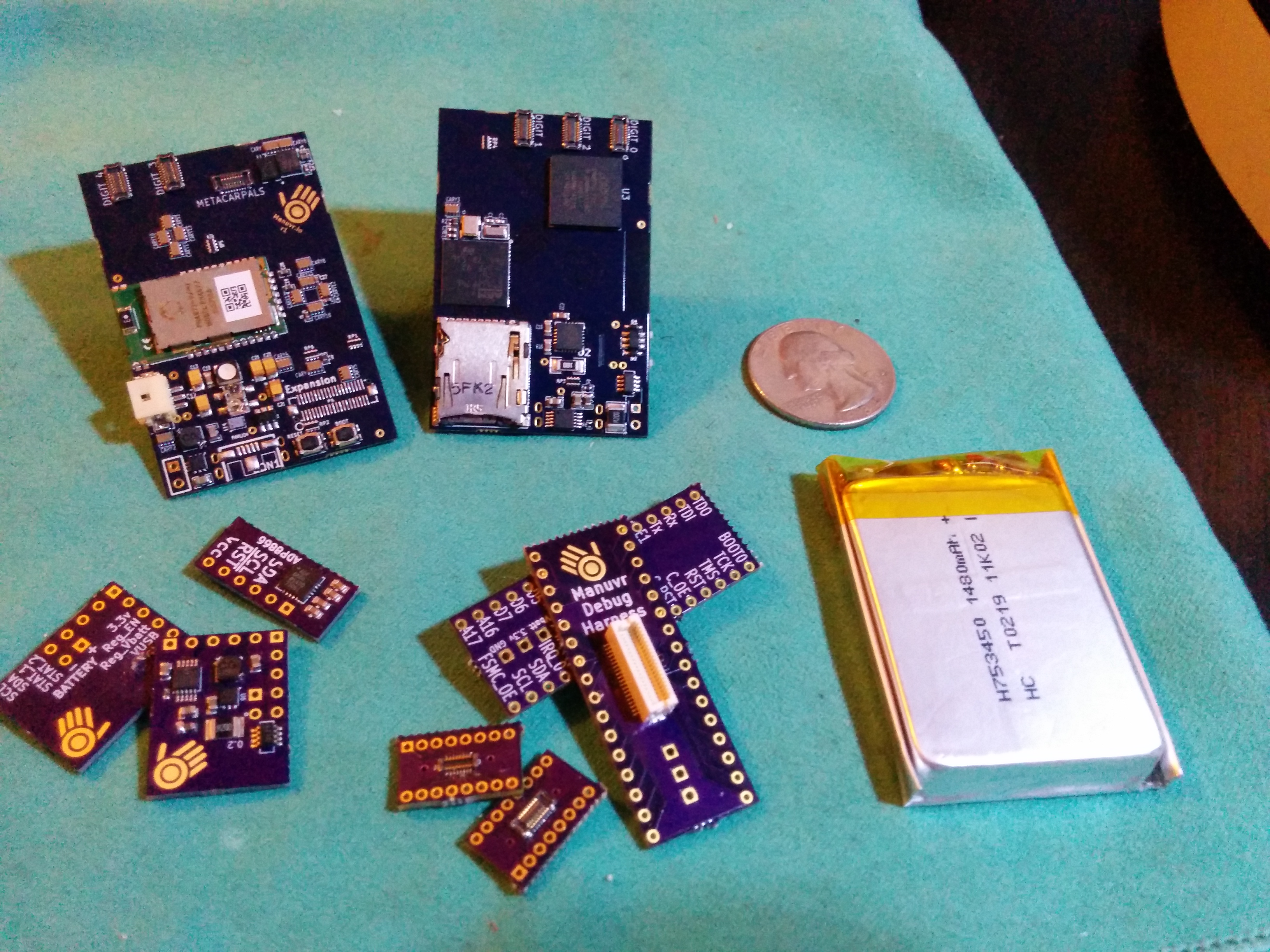
Clockwise from the US quarter...
- The chosen battery for r1.
- The r1 debug harnesses.
- The three test boards for the power subsystem on the main board. These are to be used in a separate project, now that the subsystem has been vetted.
- Digitabulum r1 main PCBs, fresh from Camtech. The subject of this post.
Major Features of the PCB
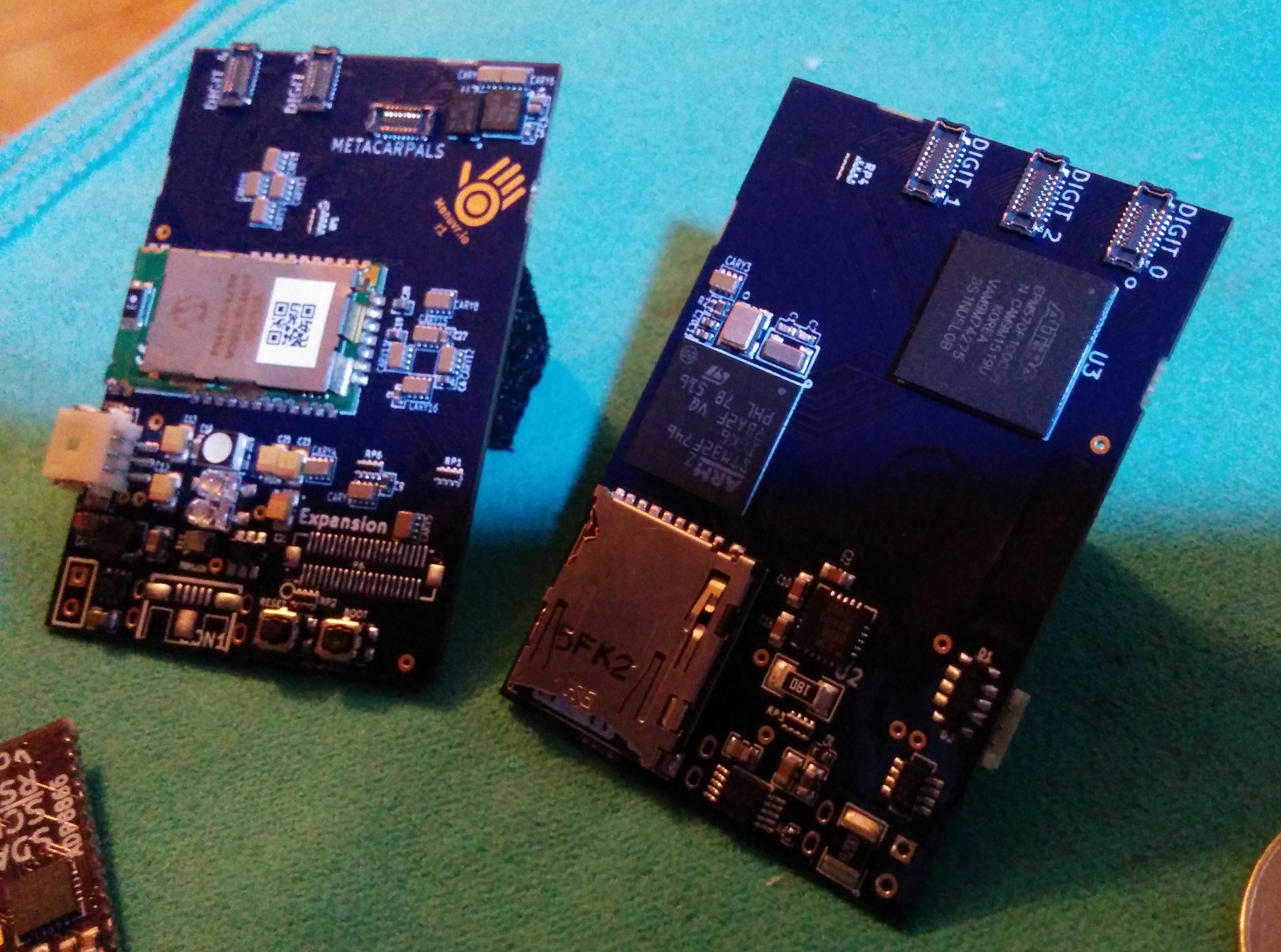
Dorsal surface on the left, ventral surface on the right.
All digit connectors are visible in this image. Three on each side. The sixth connector is for the metacarpals position. The ordering might appear random, but this order was chosen to make the design achiral without requiring different connection order for a left and right hand. The hardware fully supports runtime chirality assignment without a differential cost for left versus right handed usage.
Issues surrounding the IMU
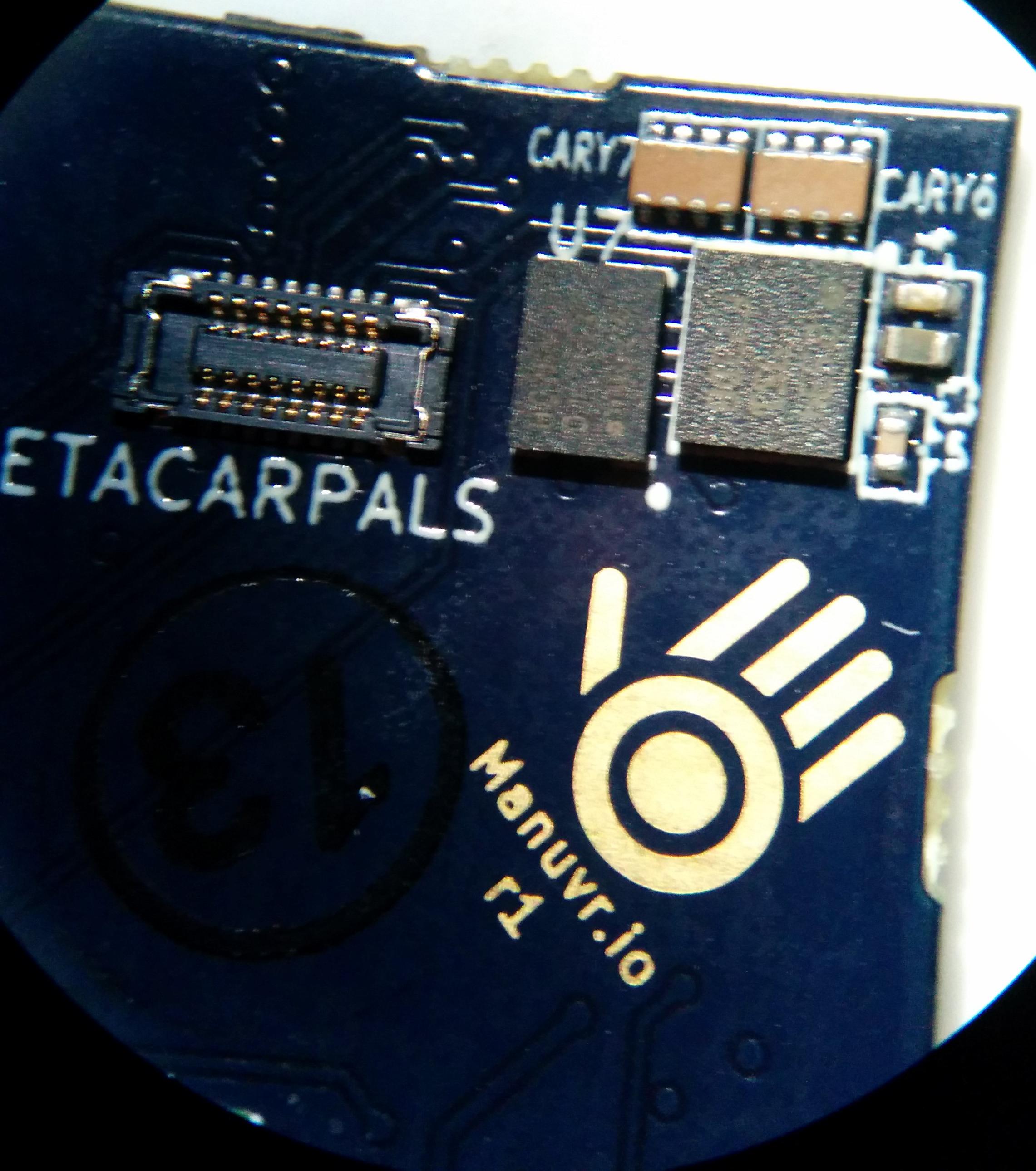
In this view through the stereoscope is the IMU for the wrist position, the connector for the metacarpals position, and our logo and hardware revision.
Care was taken this time around to keep the orientations of the IMUs correspondent to their internal organization. This saves me the trouble of spending software time converting to a consistent coordinate system (as I did in r0). It also saves the space in the CPLD that would have been required to do the same task in hardware.
The corner of the PCB was chosen for the mounting location to minimize magnetic interference. As was the case for r0, we have strict keep-out regions on all copper layers under the IMU to avoid the problems ControlVR experienced with transitory currents in ground planes causing unpredictable magnetometer readings.
Dorsal surface
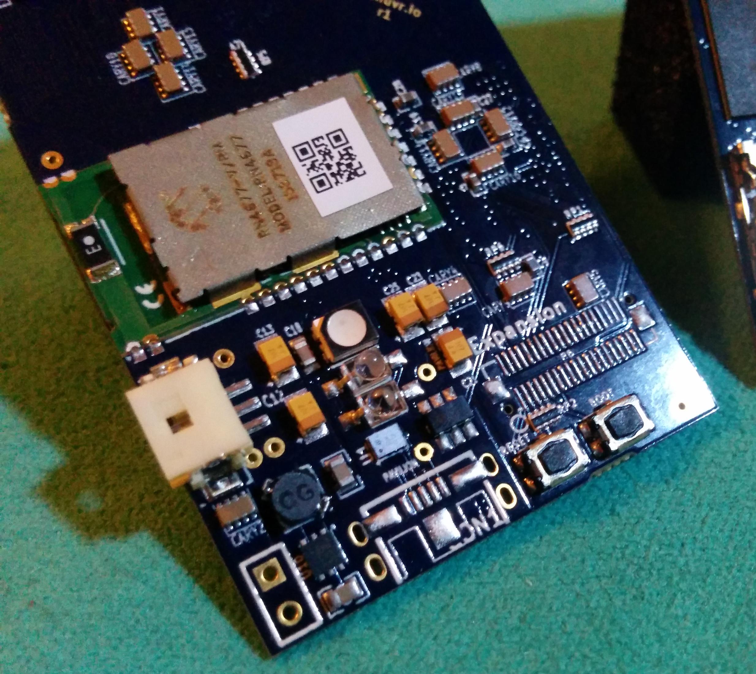
The dorsal surface of the PCB has the bluetooth radio (a Microchip RN4677), the high-current port, and the battery terminals. The IR and RGB LEDs are near the center of the board.
Reset and bootloader access buttons are on the bottom edge, along with the (absent) expansion and USB ports. More about that later.
Elements that have impulsive current-draw were placed very near the PSU (lower-left corner) with ample decoupling capacitance and pavilions to minimize ripple/noise in the power planes. That includes the microSD card, LED driver, and the high-current port.
The high-current port is the tallest part on the board, and it may be changed in the release version for that fact alone. Under the port are the switching transistors and flyback diodes. The intention was to support driving a pair of vibrator motors for a haptic wristband, and design measures were taken to ensure that this would not put inductive stresses on the semiconductors, nor introduce noise back into the power planes.
The LEDs, expansion port, and push buttons needed to be on the dorsal surface, since the ventral surface is facing the battery and body.
Ventral surface
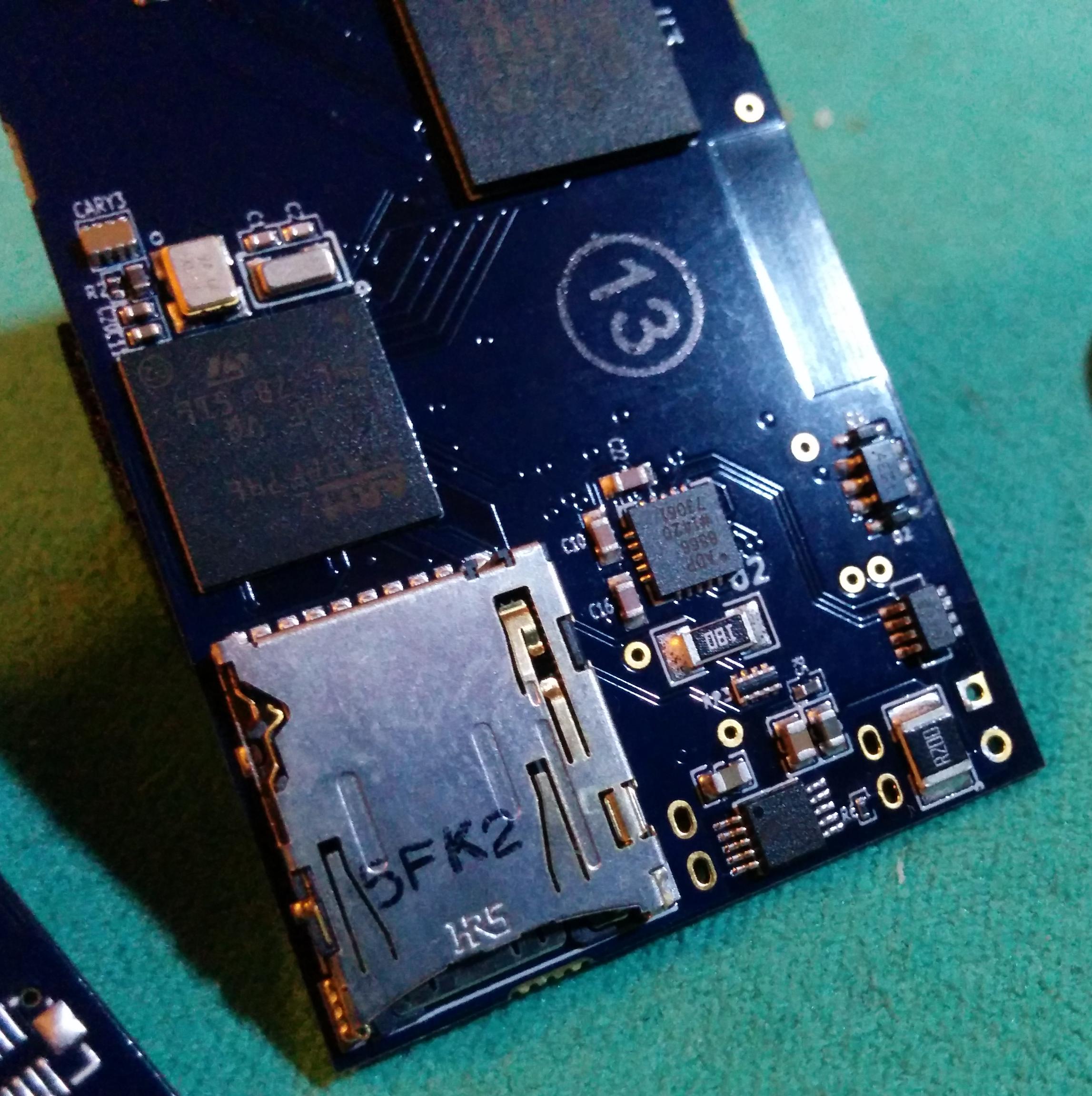
The ventral surface of the PCB is dominated by the microSD socket, above which is the STM32F7 CPU and associated oscillators. At the top of the image is the CPLD. In r0, this part was located on a separate metacarpals PCB to reduce the amount of interconnect that the main PCB needed to service. By moving to BGA parts and using via-in-pad, we were able to increase the PCB density enough to comfortably support all the digit interconnect.
It might appear that there is lots of vacant PCB on the ventral surface, but I assure you: it is being used. The area distal from the CPU is mostly occupied by interconnect signal routing on 4 of the 6 layers. The route density is, in fact, highest in this particular area.
The vacancy that lies to the right of the CPU is truly vacant. There is very little routing on any layer. This is because the bluetooth transceiver is on the opposite side. One of the worst problems with r0 was the bad layout of the PCB surrounding the RN42 which caused a non-negligible fraction of the RF output from the radio to be dumped uselessly into the board's power planes. In r1, strict adherence to Microchip's application notes regarding PCB layout demanded this slack.
Near the upper-right corner of the SD socket is the ADP8866 LED driver. r0 used the LDS8160 for this task. I was disappointed with the LDS8160, as it only had 6 LED outputs and 3 PWM channels. This meant that the brightness of the LEDs were not truly independent. Moreover, r1 now runs the LEDs directly from the battery without burdening the regulator and incurring the consequent losses and noise for this high-current subsystem.
Two placement mistakes
Prior to the boards being assembled, I noticed three footprint mistakes that affected two components. All mistakes were rectified in the CAD files for the next run. For now, I will need to manually place both parts.
This is where the expansion/debug port header should be.
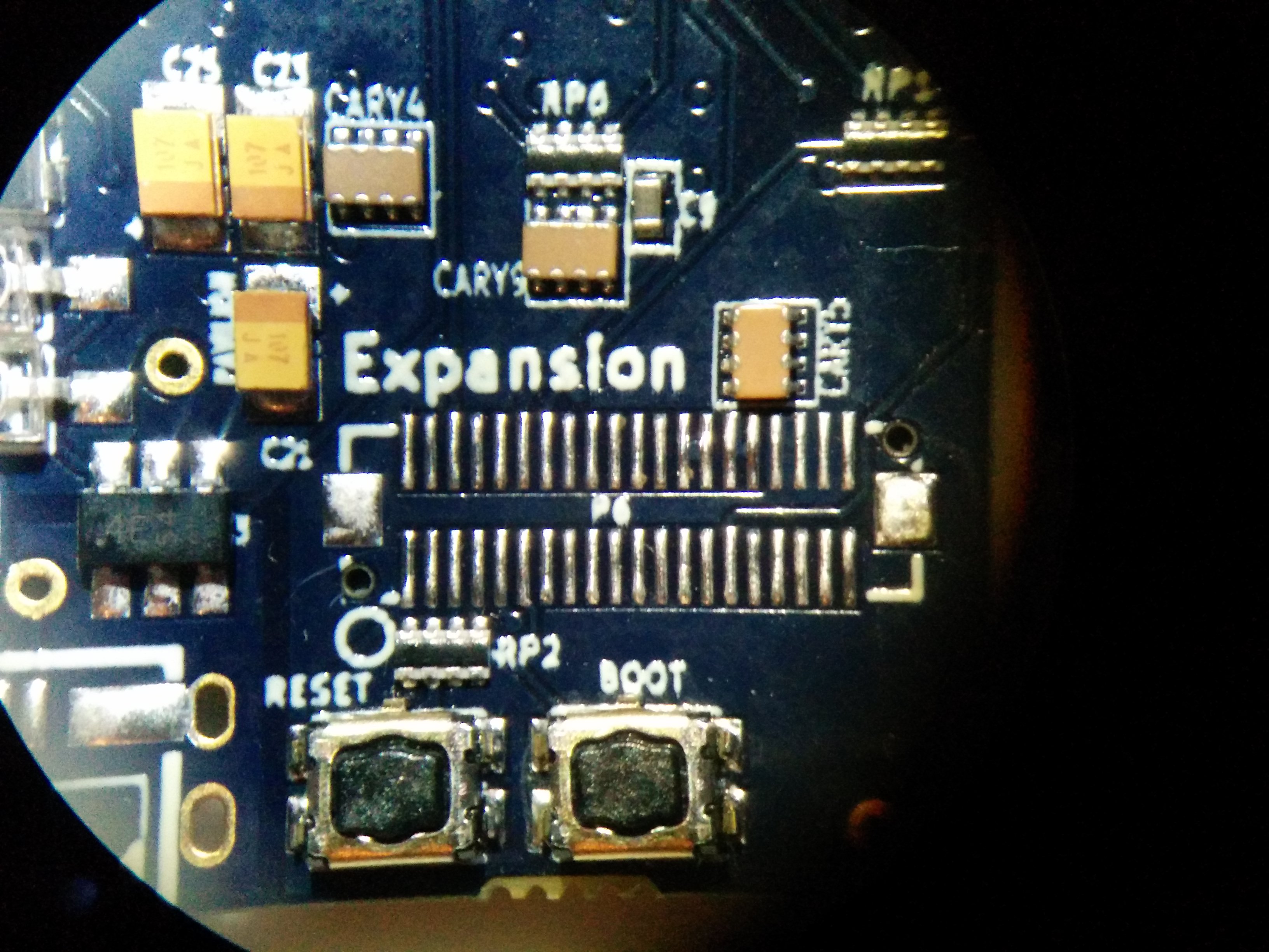
This was the worst mistake. Fortunately the pitch of the pads is accurate as is the length. But the row-to-row spacing was off just enough to make automated pick-and-place sketchy. Also, the mechanical registration holes on the part are colinear, not diagonally opposite as my footprint was (upper-right/lower-left).
RP2 and CARY5 make this repair more challenging. I would estimate this as difficulty 6/10 (assuming I don't cause collateral damage during the repair). I will need to shave one of the registration pegs off the component.
This is where the USB port ought to go.
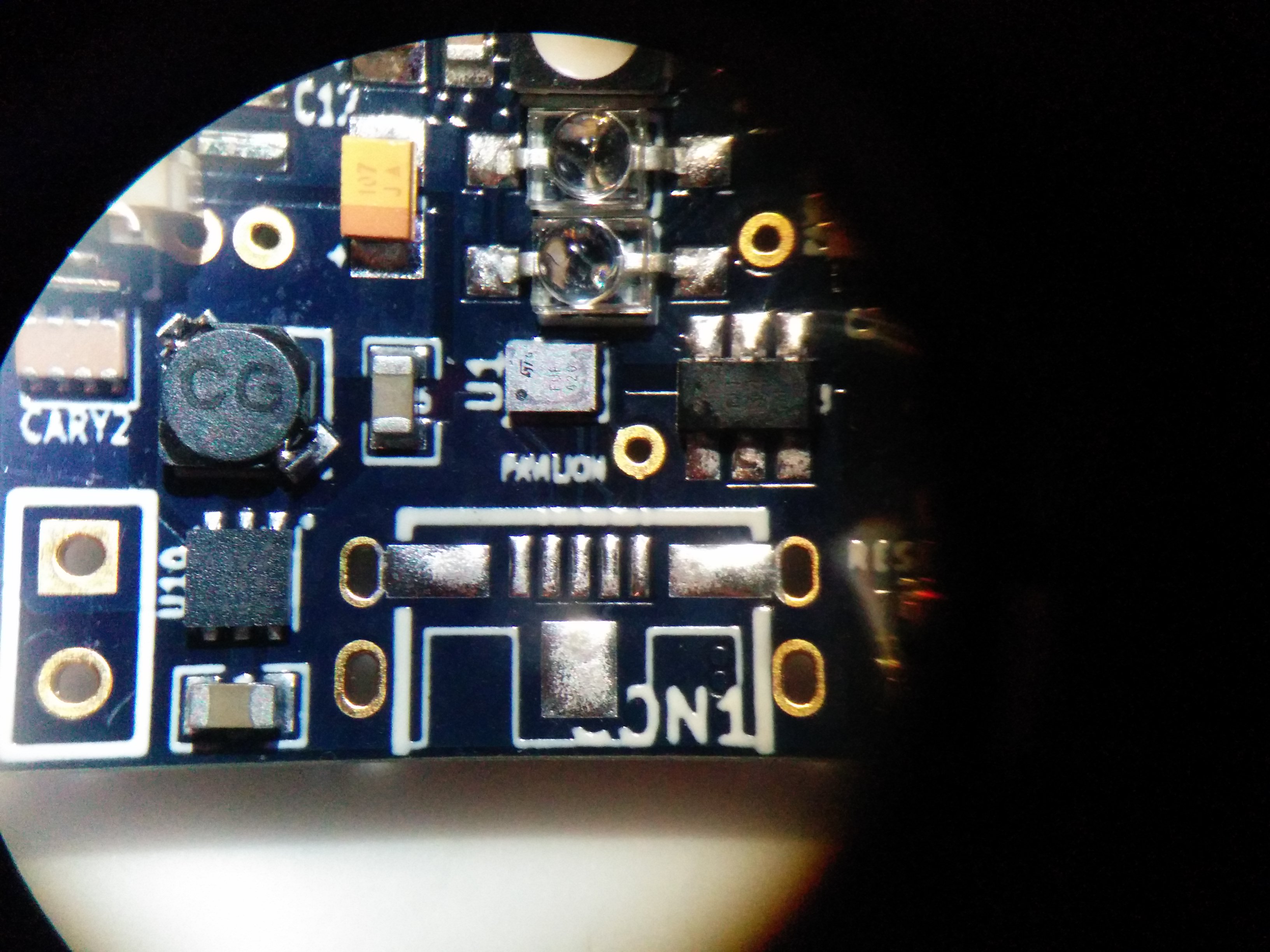
In this case, I neglected to have the PCB routed to include the notches that the silk-screen indicated. The sad thing is: This is the same USB connector used on r0, and I didn't make this mistake then.
Difficulty? 4/10. Mostly because I have to "modify" the connector with a razor blade under the microscope. Placement was trivial on the test board.
Flying uncomfortably close to the sun...
Not technically a mistake. But too close to the edge for comfort. The release version will have the PCB edge extended slightly such the the connectors fall entirely within the PCB footprint.
