We've not been making many posts the past two months. We've been hard at work on r1 and MHB (Manuvr Host Bridge).
But today is special. We got the first run of PCBs from the manufacturer. The bluetooth radio is back-ordered until the end of the month, so assembly will have to wait until then. But for now, I can give some high-level overview of the main unit's PCB.
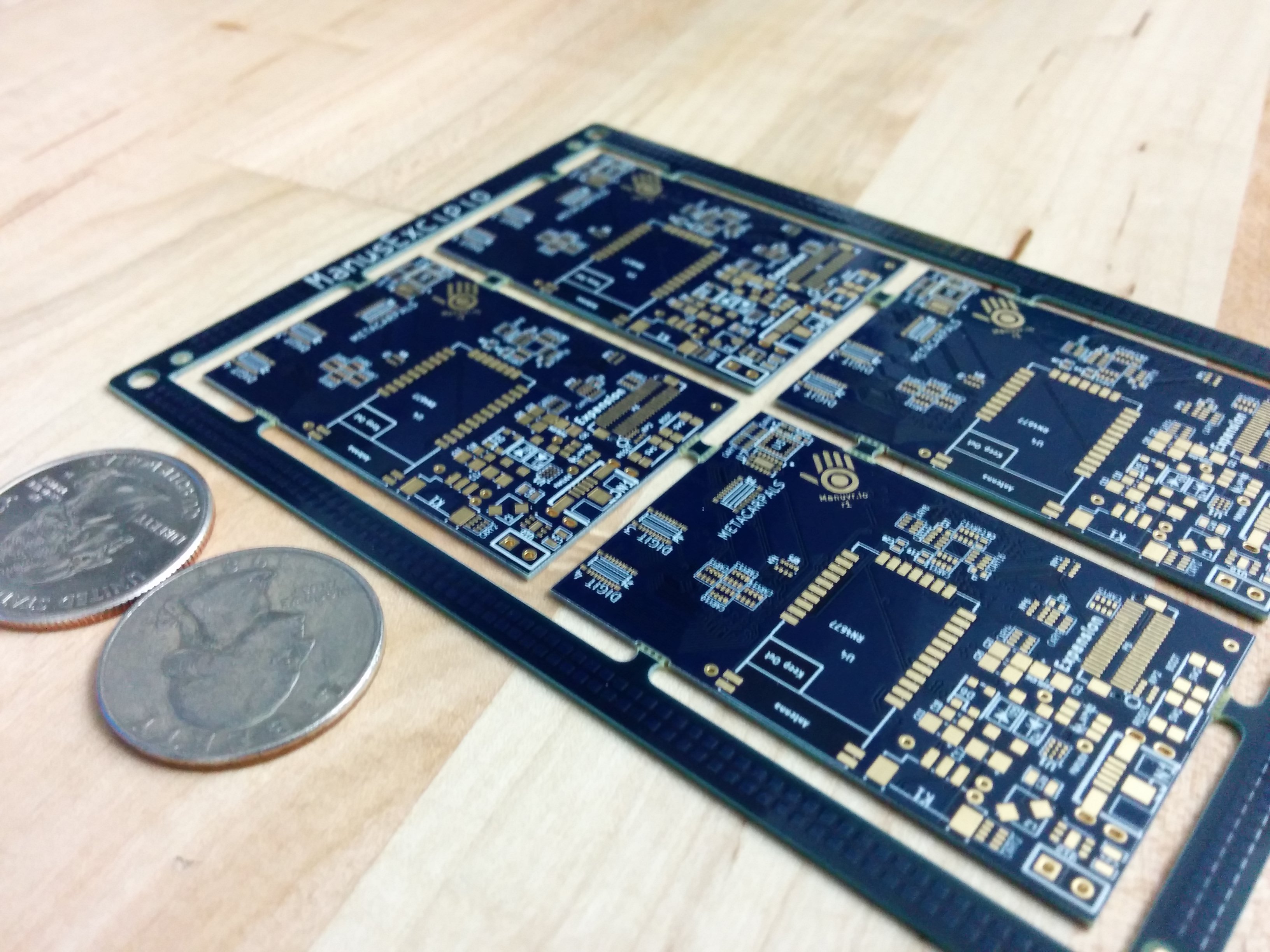
This is the full panel. The ventral surface of the PCB is visible alongside two US quarters for scale (I did not have a banana). The large BGA parts are the CPU and CPLD. The tallest feature on this surface is the microSD socket.

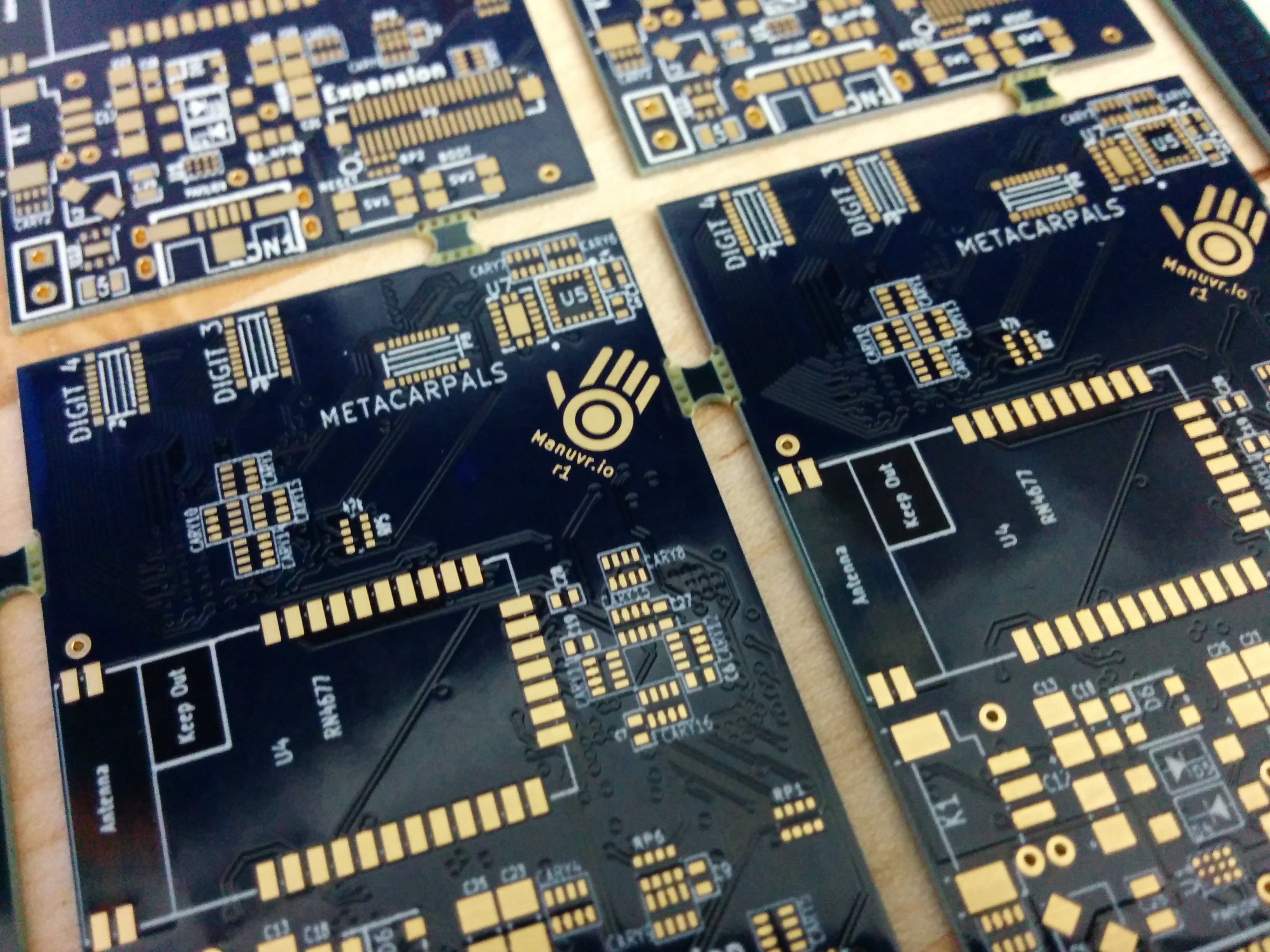
And the other side of the panel...

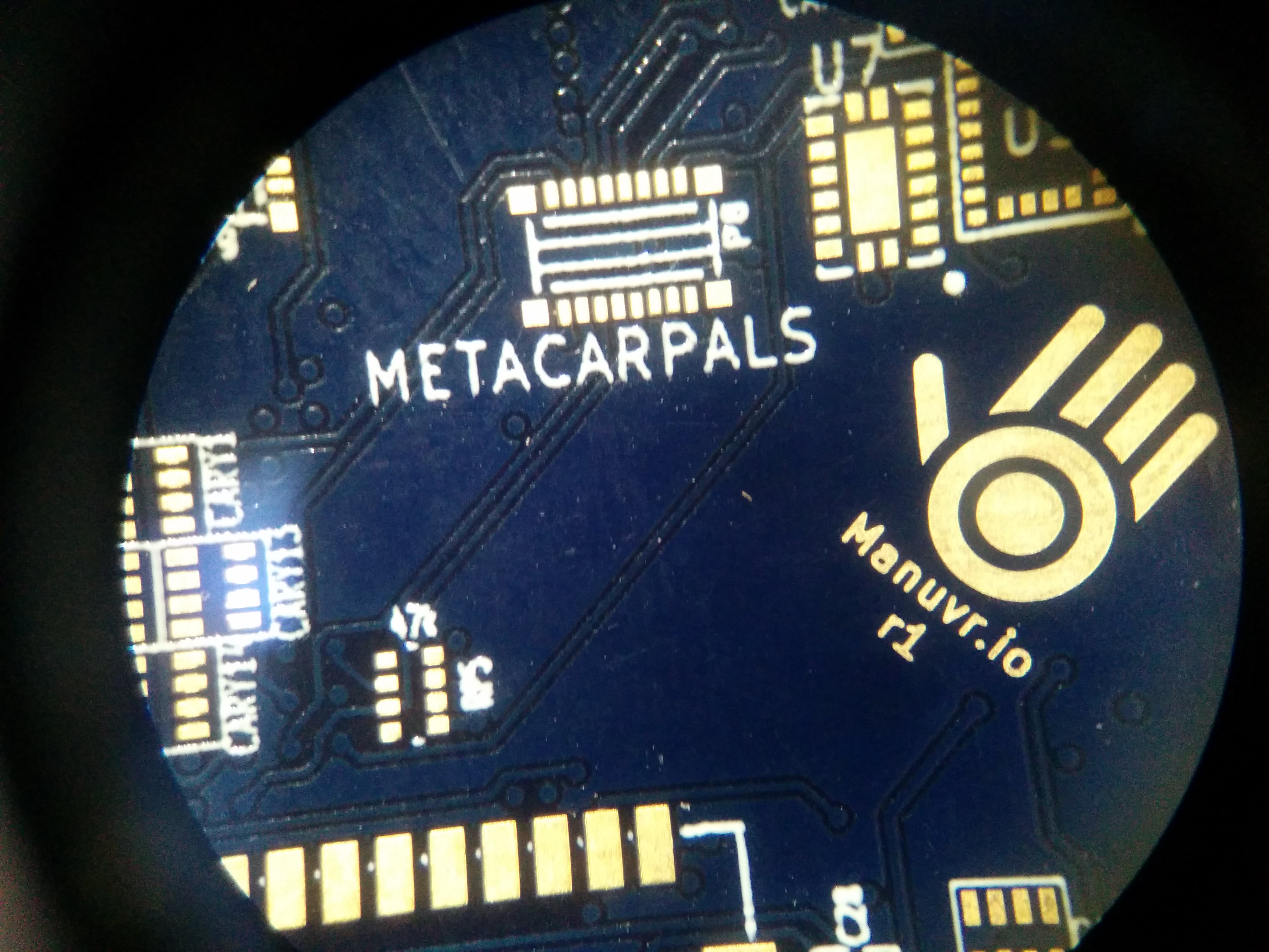
A close-up...

Our logo is so awesome...

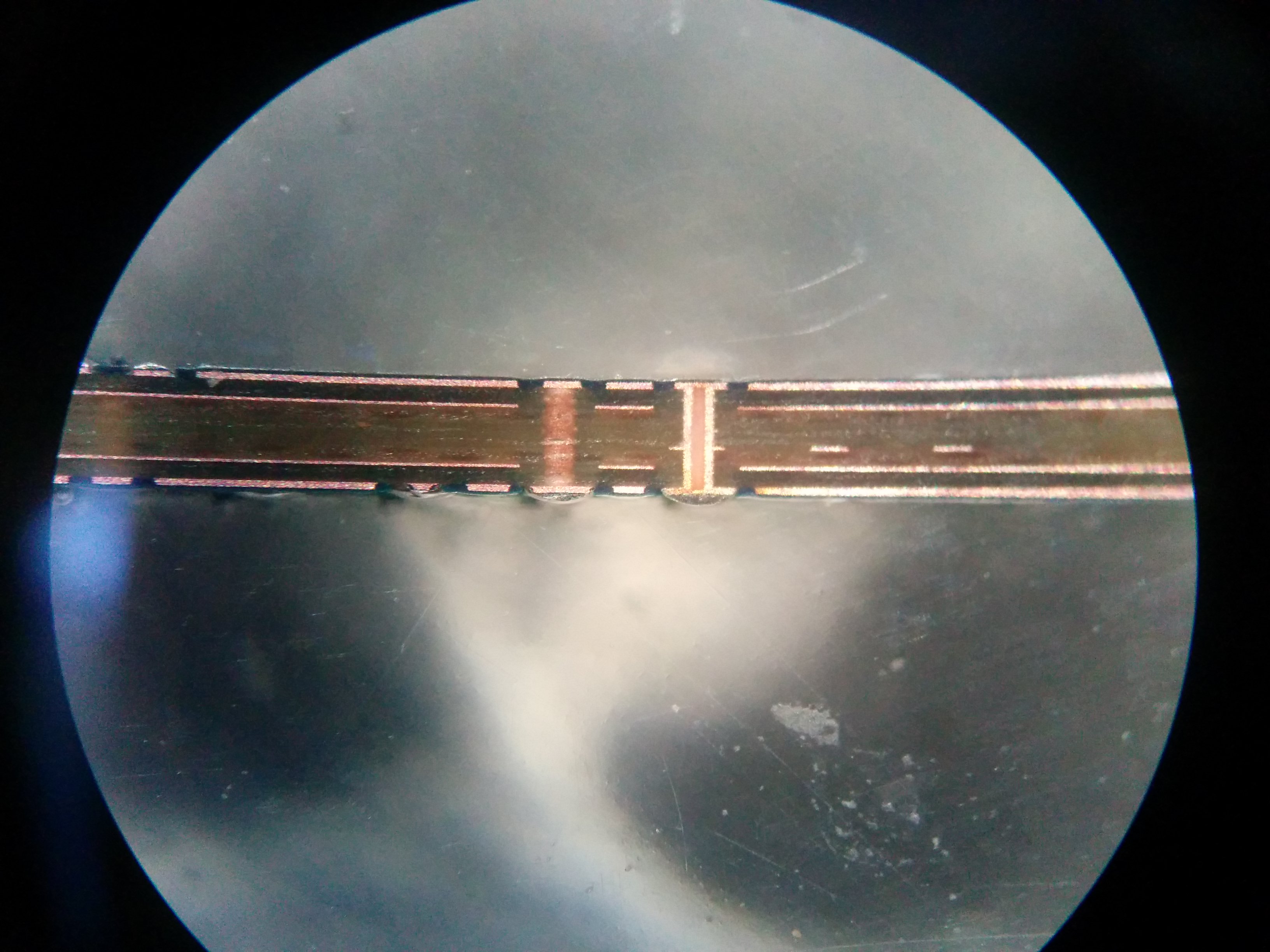
And here is a cross-section of the PCB under 30x magnification. For reference, the PCB is about half the height of a US quarter. So figure these vias are tiny. To maximize density, the vias are embedded in the pads they connect to wherever possible.

I'll write more about the PCB design once the populated copies show up.

